Your First PCB Using Fusion 360
We’ll be designing a board to replicate one of the circuits from Sensors and Circuits, specifically the BJT timer circuit.
Creating the Schematic
Importing a Schematic
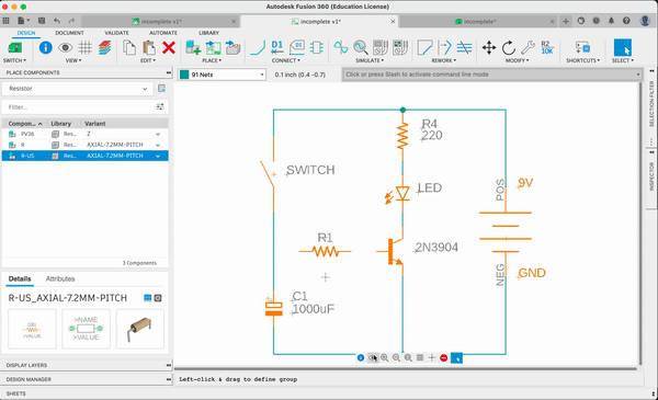
Instead of starting from scratch, we can modify an existing schematic. Download the incomplete schematic from here and add it to a Fusion electroncis design.
Once you have downloaded the file you want to click on Reference to a Schematic document, and select incomplete.sch. 
Add Parts from Resistor Library
Your schematic should look like this, but it is missing a resistor. We will use the internal parts library to find a resistor and place it in our schematic.

Click on the add part button.

On the left side of the screen there is a menu for placing components. First thing you should do is convert that menu into a tab so you can actually see what you are doing. Fusion makes it shamefully tiny and cramped by default.
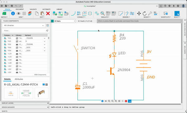
Click on the dropdown menu to select the Resistor library. Each component is comprised of two parts: a schematic symbol and a physical footprint. The schematic symbol is supposed to represent how the part functions theoretically, while the footprint is how the part actually looks on a board. You can make your own components by making the schematic symbol and footprint, but it is a tedious process and outside the scope of this tutorial. Select the R-US component and the 7.2mm pitch from the drop down menu. These are the schematic symbol and footprint, respectively.
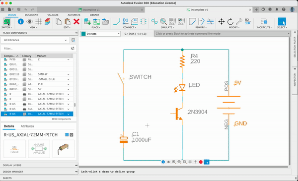
Double-click on the component in the library tab. You will notice that the component now shows up on your cursor in the main workspace. Left click to add the part to your schematic and press escape when you are done. If you are using a mouse, right click will allow you to rotate the part 90 degrees. If you are using a trackpad, you should consider making better life choices.
Connect Parts
Once your part is placed, you will need to connect it to the other components with nets. On the top ribbon, select Net. Click on either end of the part, and click to start the net. Click on the other piece you wish to connect to finish the net.
Creating the Board
Create Your Board Outline
By default, Fusion will create a rectangle for your board, but it is rather large. We can reduce the size by clicking and dragging or by changing the start and end points. Fusion also allows you to pull in a board outline from a 3D shape, but that is outside the scope of this tutorial.
Note: There are two units most commonly used in PCB design: mm and mil. Those may seem like they are the same, but mm is millimeters and mil is milli-inches (machinists call them “thous”). The practice of using decimals and prefixes can be applied to imperial units just as easily as metric ones.
Note: If this is your first iteration, you should make the board bigger than it needs to be to simplify routing and soldering. Manufacturing this bigger board in the Prototyping Labs is a great way to test whether you have your schematic right before shrinking the board and ordering from a PCB manufacturer.
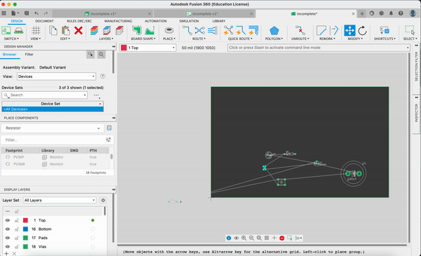
Place Components
We will be making this board all on one side to simplify soldering. You can move components by clicking and dragging them around. Note that you will need to click the origin of the part to select it (denoted by a small + sign).
When placing your parts, pay close attention to the wires connecting them. Those wires are called air wires and indicate which parts need to be connected together with traces. To make routing the traces easier, try to keep air wires from crossing each other.
Note: Your part placement will not necessarily imitate their placement on your schematic. The schematic represents how your parts interact together theoretically, but the board is just meant to connect them electrically in an efficient way.
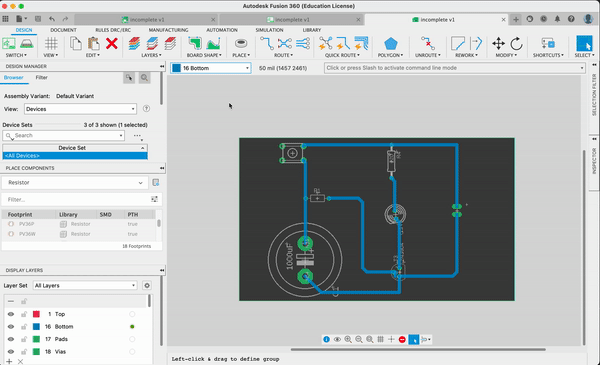
Route Traces
Since our components on the top, we will do all of our routing on the bottom of the board (blue). First, let’s change the layer to Bottom and change the trace width to 40 mil.
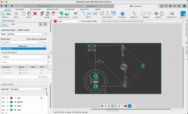
If you have trouble keeping all of the traces on the bottom layer, try rotating or moving your parts. If your traces have right angles, electrical engineers might make fun of you, but it will work for our purposes. Removing right angles becomes important when working with higher frequencies.
Export gerber files
Most PCB manufacturers use what are called gerber files. These are actually a zipped folder containing several files that define the geometry of each layer of your board (top copper, bottom copper, soldermask, silkscreen, drills, etc). Under the Manufacturing tab, select the drop down from the Manufacturing portion of the ribbon and select Export Gerber, NC Drill, Assembly, and Drawing Outputs